Detailed Process Flow Of PCB Production (1)
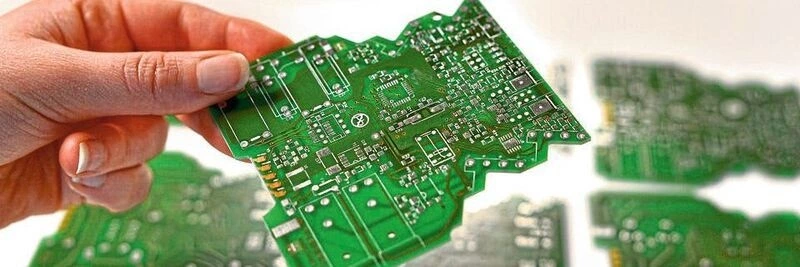
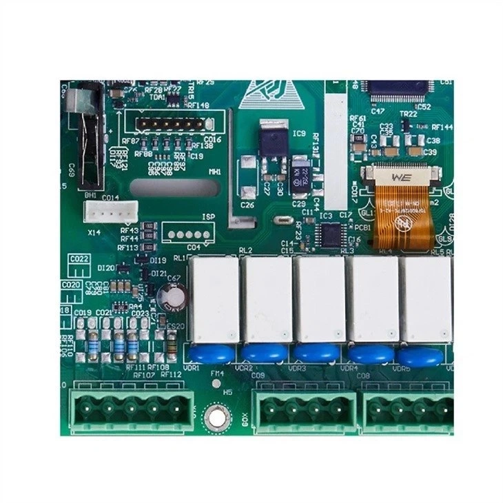
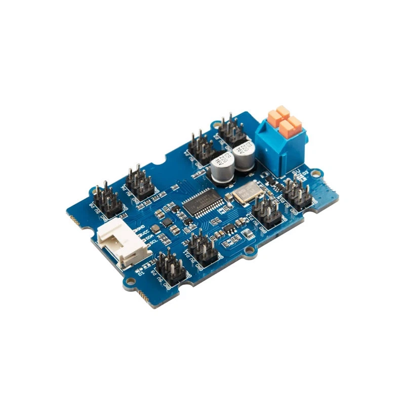
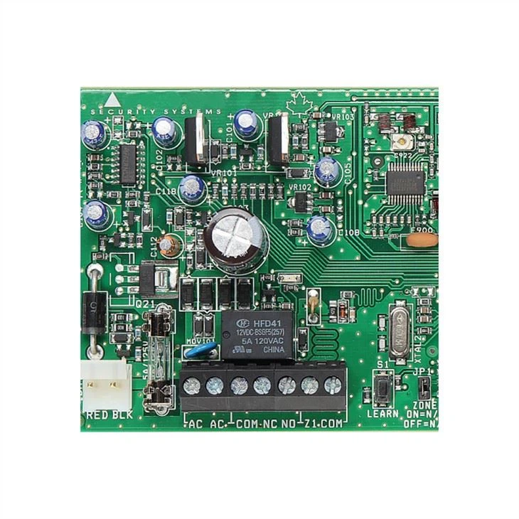
What are the technological processes of PCB board making? PCB circuit boards are used in almost all electronic products, ranging from watches and headphones to military and aerospace. Although they are widely used, most people do not know how PCBs are produced. Next , let us understand the PCB production process and production process! The following process is the complete manufacturing process of multi-layer PCB.

One,The inner layer; it is mainly used to make the inner layer circuit of the PCB circuit board; the production process is:
1. Cutting board: Cut the PCB substrate to production size.
2. Pre-treatment: Clean the surface of the PCB substrate to remove surface contaminants.
3. Lamination: Stick the dry film on the surface of the PCB substrate to prepare for the subsequent image transfer.
4. Exposure: Use exposure equipment to expose the film-attached substrate with ultraviolet light, thereby transferring the image of the substrate to the dry film.
5.DE: The exposed substrate is developed, etched, and film removed to complete the production of the inner layer board.
Two,Internal inspection; mainly for inspection and maintenance of board circuits
1. AOI: AOI optical scanning can compare the image of the PCB board with the data of the good quality board that has been entered, so as to find the defects such as gaps and depressions on the board image.
2.VRS: The bad image data detected by AOI will be sent to VRS, and the relevant personnel will carry out maintenance.
3. Repair wire: Weld the gold wire on the gap or depression to prevent poor electrical properties.
Three,Lamination; as the name implies, it is to press multiple inner layers into one board
1. Browning: Browning can increase the adhesion between the board and the resin, as well as increase the wettability of the copper surface.
2. Riveting: Cut the PP into small sheets and normal size so that the inner layer board is combined with the corresponding PP.
3. Lamination and pressing, target shooting, gong edging, edging.
Fourth, drilling; according to customer requirements, use a drilling machine to drill holes with different diameters and sizes, so that through holes between the boards can be used for subsequent processing of plug-ins, and it can also help the board to dissipate heat.
Five, Primary copper; copper-plating the holes that have been drilled on the outer layer board, so that the lines of each layer of the board are connected
1. Deburring line: remove the burr on the edge of the board hole to prevent poor copper plating.
2. Glue removal line: remove the glue residue in the hole; in order to increase the adhesion during micro-etching.
3. One copper (pth): copper plating in the hole makes all layers of the board conduct, and at the same time increases the copper thickness.


