Processing And Precautions Of PCBA
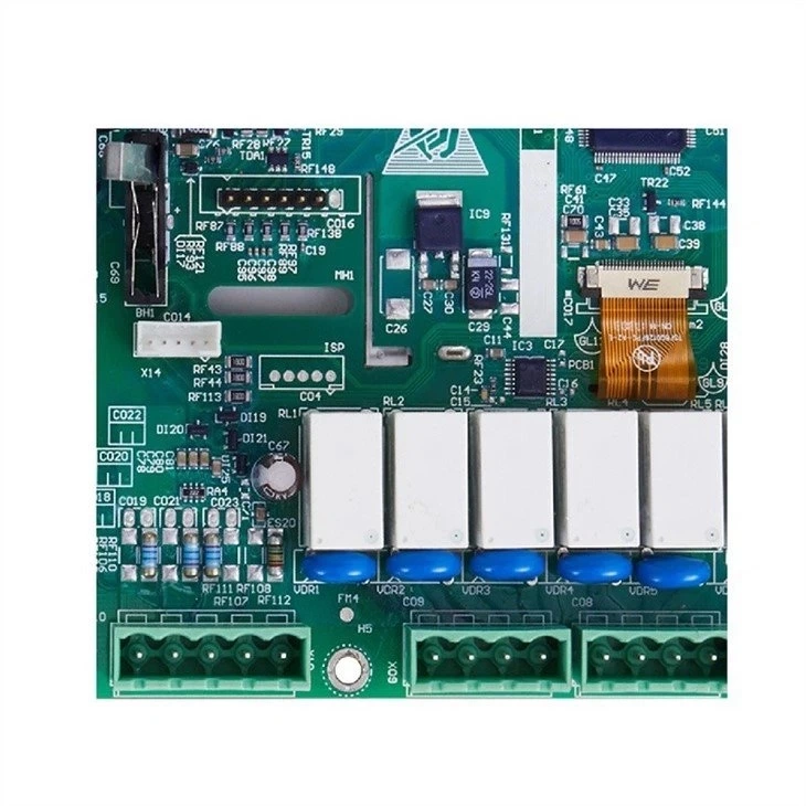
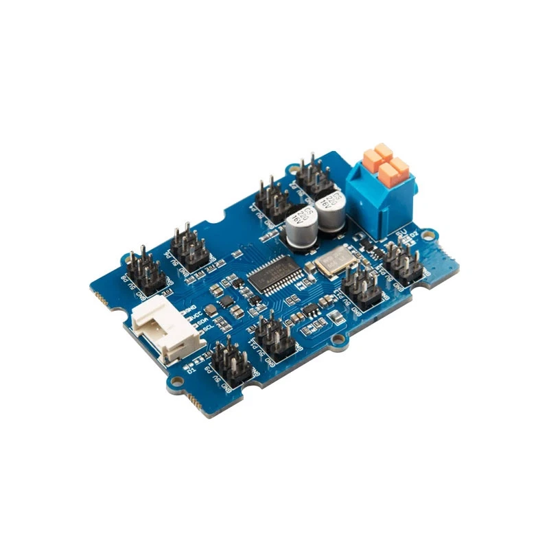
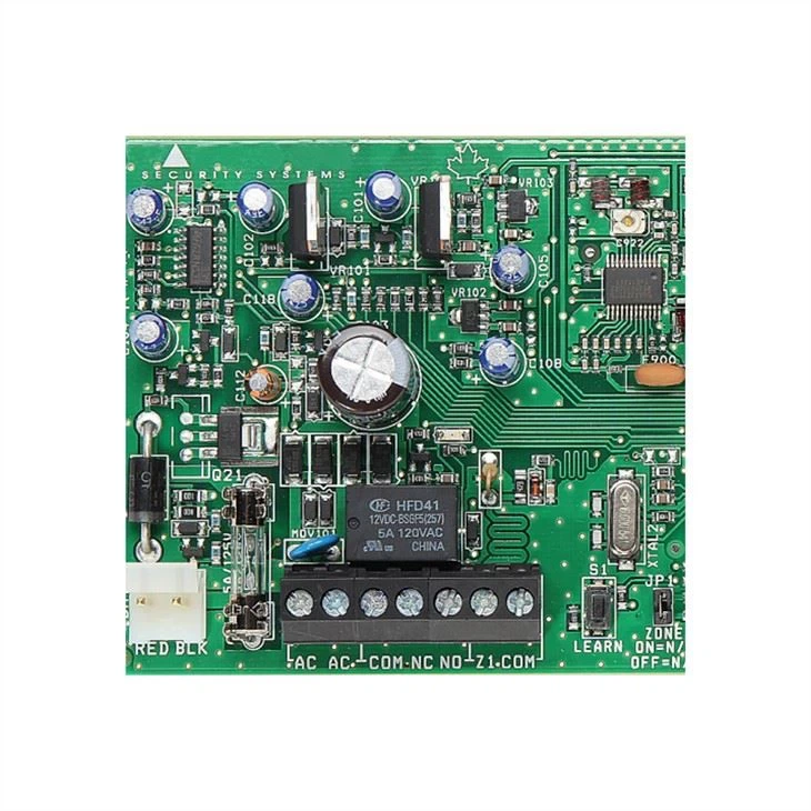
The PCBA processing process involves many links. To produce a good product, the quality of each link must be controlled. General PCBA consists of: PCB circuit board manufacturing, procurement and inspection of components, SMT chip processing, plug-in processing, program firing, testing, aging and other processes. Below we carefully explain the points to be noted in each link.
1. PCB circuit board manufacturing
After receiving the PCBA order, analyze the Gerber file, pay attention to the relationship between the PCB hole spacing and the board's carrying capacity, not to cause bending or breaking, and whether the wiring considers key factors such as high-frequency signal interference and impedance.
2. Procurement and inspection of components
The procurement of components requires strict channel control, purchases from large merchants and original factories, and 100% elimination of second-hand materials and counterfeit materials. In addition, set up special incoming inspection positions to strictly check the following items to ensure that there are no defects in parts.
PCB: Reflow soldering furnace temperature test, prohibit flying wire, whether the hole is blocked or ink leakage, whether the board surface is bent, etc.;
IC: Check whether the wire mesh is completely consistent with BOM, and maintain constant temperature and constant humidity;
Other commonly used materials: check silk screen, appearance, start-up measurement, etc. The inspection items are carried out according to the random inspection method, and the proportion is generally 1-3%.
3. SMT assembly and processing
Solder paste printing and reflow oven temperature control are key. The quality and process requirements of laser steel mesh are very important. According to the requirements of PCB, some need to increase or decrease the steel mesh holes, or use u-shaped holes, according to the process requirements to make steel mesh. The furnace temperature and speed control of reflow soldering is critical to solder paste infiltration and soldering reliability, and can be controlled according to normal SOP operating guidelines. In addition, AOI testing should be strictly implemented to minimize the adverse effects caused by human factors.
4. Dip plug-in processing
In the process of insertion, the mold design of wave soldering is the key. How to use the mold to provide the best products after the furnace to the maximum, this is the process that PE engineers must constantly practice and sum up experience.
5. Program burning
In the previous DFM report, customers can suggest setting some test points on the PCB, the purpose is to test the continuity of the PCB and PCBA circuit after soldering all components. If you have the conditions, you can ask the customer to provide a program, mainly through the burner control integrated circuit (such as ST-LINK J-LINK, etc.), you can more intuitively test various touch behavior functions to change the entire PCBA test function Integrity.
6. PCBA board test
For orders with PCBA test requirements, the main test content includes ICT (circuit test), FCT (functional test), Burn In test (aging test), temperature and humidity test, drop test, etc. Operate and summarize report data according to customer test plan.


