The Importance Of PCB Assembly Manufacturing Technology-ensuring Product Quality
How to ensure high quality PCBA board
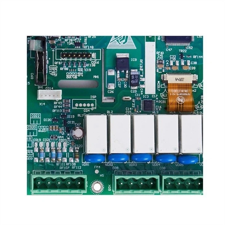
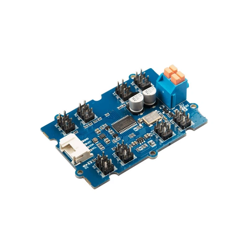
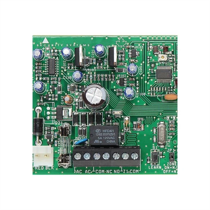
PCB assembly is a complex method of filling electronic components on a bare PCB, which is the primary condition for manufacturing functional electronic / electrical products. This can be done by automatic electronic component placement or manual / conventional placement, depending on the designer's use of electronic component technology. In this article, we will address the quality assurance of PCB components using automatic electronic component placement and how to perform them:
Automatic placement
Automatic placement refers to the process of using an automatic placement machine to place electronic components one by one on a PCB with solder paste deposited. To ensure proper placement of electronic components, each electronic component to be installed must be properly taught and programmed before running the automatic placement program. Failure to do so may result in placement accuracy issues and ultimately problems such as missing components and incorrect placement.
Wave soldering
Wave soldering is a soldering method very similar to hand soldering, but this time an automated machine was used, in which the PCB was subjected to a molten solder bucket, causing the solder to flow through the intended PCB holes. Usually used for PCB designs with a large number of electronic components using through-hole technology. To ensure that the proper amount of solder flows through the PCB holes, an appropriate wave solder reflow profile must be performed.
Wave soldering adopts a special design in order to eliminate the "shadow effect". For example, it is best to arrange the components in the same direction. The connection between the two metalized ends of the chip component should be perpendicular to the direction of the wave soldering. Components and small components should be placed alternately. The long axes of SOP and SOT should be arranged parallel to the direction of tin wave flow. The length of the SMC / SMD pads should be extended. At the same time, the component pads (usually 2.0mm) should be extended to increase solder contact. Area, reducing false soldering and missing soldering.
These are just some PCB assembly processes and their corresponding precautions to ensure high quality output.
If you need PCB design or PCB assembly services, please feel free to contact us.


