Understand Spark's Damage To PCB
Semiconductor manufacturers attach great importance to electrical overload (EOS) and electrostatic discharge (ESD). First, for obvious reasons, EOS and ESD may damage parts during manufacturing, packaging, assembly, and testing. But more importantly, these negative forces will directly affect the quality and service life of the circuits in the hands of customers.
Initially, the part that is exposed to excessive electrical stress may appear to be working properly. It might even run in a slightly degraded manner, but still passed the automatic test equipment (ATE) inspection, but later failed on site. EOS and ESD failures are preventable and are undoubtedly key quality control issues.
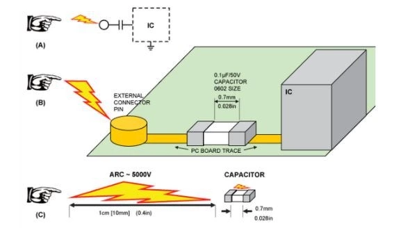
EOS and ESD damage are most likely to occur where ICs are manufactured during manufacturing. Figure A shows a schematic diagram of the PCB. We might think that the IC is protected by a series capacitor. This is not the case. The second opportunity to cause damage is for customers to mount the IC on the PCB to manufacture the product. Looking closely at Figure 1B, we can see that the capacitor has an operating voltage of 50 V, but the distance between the two metal end connections is only 0.28 inches (7 mm). Since the spark has just jumped 0.4 inches (1 cm), the small gap around the capacitor is easily damaged. The result may be IC's life (Figure C). Finally, when customers operate the product in their environment, EOS or ESD damage may occur.
Of course, there are many opportunities for huge losses. We can actually see the result of EOS and ESD damage inside the IC. For this reason, the epoxy material of the packaging must be removed. This is usually done with hot acid in a double glove box. This process is very dangerous. Smoke is deadly. One breath can lead to painful death. Putting a drop of acid on a person's skin will only cause amputation of the hand or arm, and even the most serious death.
