What Are The Methods For Circuit Board Testing And How Can Faults Be Rapidly Detected On Circuit Boards
Methods For Circuit Board Testing
1.Bed-of-Nails Testing
This method involves using spring-loaded probes connected to every test point on the circuit board. The springs provide 100-200g of pressure at each test point to ensure proper contact. These probes, arranged together, are referred to as a "bed of nails." Controlled by testing software, programming can be performed on the test points and test signals. In practice, only the probes required for testing specific points are installed. While bed-of-nails testing can simultaneously test both sides of the circuit board, it is advisable to have all test points on the soldering side of the board when designing the PCB. Bed-of-nails testing equipment is expensive and challenging to maintain. The selection of probe arrangements depends on their specific applications.
A fundamental general-purpose grid processor consists of a drilled board with pin centers at 100, 75, or 50 mil. These pins act as probes and make direct mechanical connections through connectors or nodes on the circuit board. If the solder pads on the circuit board match the test grid, standard punched polyimide films are placed between the grid and the circuit board for specific probing. Continuity testing is achieved by accessing the endpoints of the grid, which have been defined as the x-y coordinates of the solder pads. This way, independent testing is completed. However, the proximity of the probes limits the efficiency of bed-of-nails testing.
2.Visual Inspection of Circuit Boards
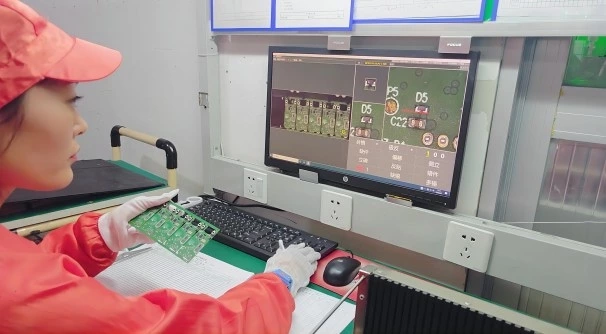
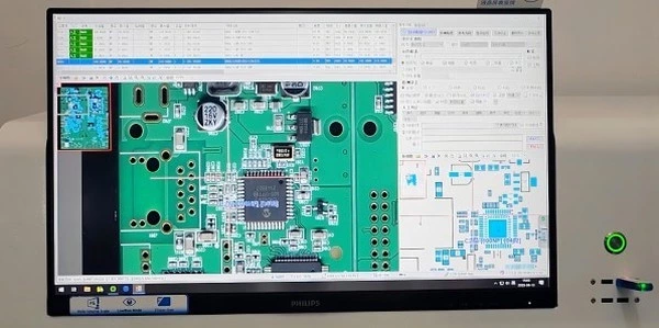
Due to the small size and complex structure of circuit boards, specialized observation equipment is essential for their examination. Typically, portable video microscopes are used for observing the board's structure. Using a video microscope camera, the microscopic structure of the circuit board can be viewed clearly and intuitively. This approach greatly facilitates circuit board design and inspection. Portable video microscopes like the MSA200 and VT101 are commonly used on factory floors due to their convenience, allowing for real-time observation, on-the-fly inspection, and collaborative discussions, making them superior to traditional microscopes.
3.Double Probe Flying Needle Testing Method
The flying probe tester operates independently of footprints mounted on fixtures or supports. In this system, two or more probes are mounted on tiny, freely movable magnetic heads in the x-y plane, with test points directly controlled by CADI Gerber data. The double probes can move within a range of approximately 4 mils from each other. These probes can move independently, with no real constraints on how close they can get to each other. Testers equipped with two movable arm-like devices are based on capacitance measurement. The circuit board is placed firmly on an insulating layer on top of a metal plate, serving as the other plate of the capacitor. If there is a short circuit in the circuit, the capacitance will be higher than at a specific point. If there is an open circuit, the capacitance will decrease. This method is slower but remains a viable choice for manufacturers dealing with lower yields of complex circuit boards.
For bare board testing, specialized instruments are available. An economically efficient alternative is to use a universal instrument, despite the initial higher cost compared to specialized instruments. This cost is offset by reducing individual setup costs. For standard grids, the standard grid for leaded components and surface-mount device standard grids is 2.5 mm. In this case, the test pads should be larger than or equal to 1.3 mm. For Imm grids, the test pad should be designed to be greater than 0.7 mm. If the grid is smaller, the test pins become smaller and more fragile, making them susceptible to damage. Hence, it is advisable to opt for grids larger than 2.5 mm. Combining a universal tester (standard grid tester) and a flying probe tester ensures precise and cost-effective testing for high-density circuit boards.
Another recommended approach is the use of a conductive rubber tester, which can be employed to detect points deviating from the grid. However, variations in the height of solder pads due to hot air leveling treatment may obstruct the connection of test points."

Why can Tecoo provide complex PCB Assembly manufacturing services? We not only have high-end production capacity but also reliable testing methods.
How to Quickly Detect Faults on a Circuit Board?
- Examine Component Status
When dealing with a faulty circuit board, the first step is to visually inspect for obvious component damage. This includes checking for burnt or swollen electrolytic capacitors, burnt resistors, and damaged power devices.
Inspect the Circuit Board's Soldering
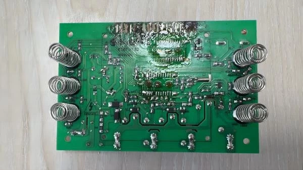
Look for signs of deformation or warping in the printed circuit board. Examine solder joints for any signs of detachment or obvious solder bridges. Check if the copper foil on the circuit board has lifted or turned black due to scorching.
- Check Component Orientation
Ensure that components like integrated circuits, diodes, and power supply transformers are correctly oriented and inserted.
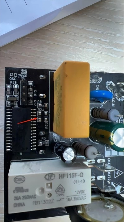
Electronic Components Missing
- Perform Basic Testing of Resistors, Capacitors, and Inductors
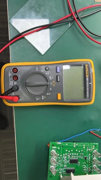
Use a multimeter to perform basic testing on components suspected of issues within its measuring range. Look for indications such as increased resistance, short-circuits, open-circuits, and changes in capacitance or inductance.
- Conduct Powered Testing
If the issues cannot be resolved through the initial observations and tests, proceed to powered testing. Start by verifying the proper functioning of the power supply on the circuit board. Check for abnormalities in the AC power source, regulator output, and the output waveform of switching power supplies.
- Reprogramming
For boards containing programmable elements like microcontrollers, DSPs, CPLDs, consider reprogramming them to eliminate potential circuit faults resulting from abnormal program execution.
- Segment-Based Repairs
If the above steps do not yield a resolution, you will need to identify the faulty circuit module based on the circuit fault and further repair it following the design schematics.
